With chip computing capacity increasing faster than ever, the industry is looking to pack more chips together. Silicon Box might have that answer better than others.
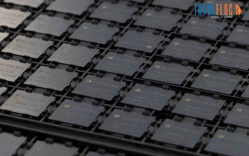
Singapore-based Silicon Box has an ambitious mission statement: it wants to disrupt the semiconductor industry by easing the supply chain bottleneck that has plagued the industry since the COVID-19 pandemic. To achieve that, it plans to fit square chips on square panels, a radical departure from the standard practice of fitting square chips on circular panels.
Currently, square chips are placed on circular wafers measuring 300nm. The industry has traditionally placed chips on wafers because wafers are the foundation of the semiconductor industry, with most tools and machines designed to work on them.
Yet, with the current spike in demand for powerful chips for advanced AI systems, packaging these chips on wafers has become the bottleneck. Moreover, a fundamental flaw with circular wafers is that the space on the wafers cannot be fully utilised. This is why there is growing interest in utilising the space available on wafers more efficiently to produce more powerful chip systems.
Silicon Box’s approach to advanced packaging with square panels at scale has seen a surge in demand. According to Dr BJ Han, co-founder and CEO of Silicon Box, despite the company’s relative newness, it already ships hundreds of products, with more than a billion shipments touted for this year. In the first quarter, its revenue is already 75% of 2025 levels, with booked order production volume increasing 10- to 12-fold from 2025 levels. It has raised $658 million at a $1.55 billion valuation.
From Ideating to Manufacturing: A 40-Year Journey
Dr Han, Dr Sehat Sutardja, and Weili Dai, friends since before their university days, had been dreaming of collaborating to revolutionise the semiconductor industry as early as the 1980s, when the three graduated from their respective institutions. However, the three would spend more than 30 years in their respective fields before co-founding Silicon Box.
In 2021, Dr Han wrapped up his 20-year career at STATS ChipPAC, a Singapore-based integrated circuit manufacturing and technology services provider, to join Dr Sehat and Weili to fulfil their lifelong dream of making a collaborative platform that would unify chip designers, Outsourced Semiconductor Assembly and Testing (OSAT) units, foundries, and various stakeholders to create a “true chiplet ecosystem”. A chiplet is a tiny, modular semiconductor integrated circuit that performs a specific function.
In March 2022, Silicon Box secured a $51 million SAFE funding round, and in July, Silicon Box broke ground on its flagship 73,000-square-metre facility, which includes 30,000 square metres of production space. Yet the concern was that there were no startups in semiconductor manufacturing due to its capital-intensive nature. Dr Han would later admit that they were a bit ‘naive’ to foray into the space only because they ‘knew too much about it’, but were also confident that they could build something.
Their confidence started yielding results the next year, when it closed a $156.6 million Series A funding round, with Tata Electronics joining as a strategic investor, along with VC firms BRV Capital and Ignite Innovation Fund. It also inaugurated its state-of-the-art semiconductor integration facility in Singapore, built with a total investment of $2 billion.
In January 2024, Silicon Box turned a unicorn when it raised $202 million in a Series B funding round to expand its chiplet technology globally to support the development of LLMs, generative AI, mobile computing, and automotive tech. Silicon Box announced in March 2024 that it will invest $3.5 billion to establish a chiplet-based integration facility in northern Italy to provide advanced packaging and test capacity.
Advanced Packaging for AI Chips: The Next Frontier
The AI boom has increased interest in advanced chip packaging due to improved material efficiency and efforts to avoid wasting space on wafers. According to market research firm Yole Group, the advanced packaging market is expected to reach $79.4 billion in 2030. Industry observers claim that traditional transistor scaling is slowing down, and the chipmaking industry is now looking at a different approach to improve performance, which is where advanced packaging comes in.
Silicon Box has a massive opportunity to tap into the AI space if it can successfully scale its advanced packaging offerings. But because there is demand for advanced packaging solutions, other companies are investing in this space as well. Vertically integrated wafer foundries such as TSMC, the world’s largest contract chipmaker, are also investing in panel-level packaging processes.
Currently, the Singapore-based company packages square chips on square panels that have more than six times the productive area of a standard 300 nm circular wafer. According to Yole Group, Silicon Box is one of the promising startups in the panel-based process, and credits the reputation and expertise of the three co-founders for its ability to attract investors and customers. Silicon Box’s success could also give Singapore’s semiconductor industry greater exposure to the leading-edge manufacturing segment.